Tracking the information about your manuscript
Communicate with the editorial office
Query manuscript payment status Edit officeCollecting, editing, reviewing and other affairs offices
Managing manuscripts
Managing author information and external review Expert Information Expert officeOnline Review
Online Communication with the Editorial Department
Editor-in-chief

LIU Yichun
Academician of Chinese Academy of Sciences,

WeChat official account
About the Journal
 Chinese Journal of Vacuum Science and Technology (CJVST) is national level scientific journal operated by the Chinese Vacuum Society and approved by the Chinese Association for Science and Technology. CJVST pressed the first volume in 1981. Since then, CJVST has been listed as a Chinese Science Citation Database (CSCD) journal and Chinse Core Journal. CJVST publishes Chinese and English research papers on vacuum acquisition, improvement, testing, and application, involving the intersection of physics, chemistry, engineering, materials, biology and other disciplines.
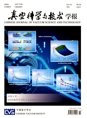
Cover Aticle
Thermal Optimization Analysis of a Two-stage Anode Layer Hall Thruster
Cathodic Cage Plasma Nitriding Technology and its Application in Material Surface Modification
Development of Vacuum Chambers for the Arc Section of HEPS Storage Ring
Design of Air-coupled Broadband CMUT Micro-elements and Array Configurations
Secondary Electron Suppression in a Compact ECR-DD Neutron Generator
more..Pumping Performance Prediction Model and Analysis Method of Screw Vacuum Pumps
WU Jun;ZHU Wenming;HE Haibin;WANG Lei;WU Qingyun;WANG Xudi;WU Jie;With the improvement of the cleanliness requirement of vacuum environment in semiconductor and other fields, dry twin-screw vacuum pumps are widely used due to their oil-free and high ultimate vacuum characteristics. The theoretical prediction of the pumping performance of screw vacuum pumps is realized through numerical modeling, which is the key to the research and design of screw vacuum pumps. The existing chamber model for pumping performance prediction of screw vacuum pumps has the problem of not being able to obtain the continuous pressure change curve. In this paper, a new “dynamic chamber model” is proposed for the pumping speed prediction of screw vacuum pumps. By comparing with the experimental pumping speed curves, it is verified that the new model proposed in this paper can predict the pumping speed performance of the screw vacuum pump more accurately, Verified against experimental data, it predicts more accurately: at 5.8 Pa(near ultimate vacuum),its 40.18 m3/h pumping speed shows a 31.5% deviation from measurements, versus the existing model's 41.63 m3/h with a 63.2% deviation. Additionally, it generates continuous pressure curves for the rotor chamber, reflecting gas transport throughout the full working cycle.
Thermal Optimization Analysis of a Two-stage Anode Layer Hall Thruster
CHEN Xingkai;LIU Chao;GUO Ning;GAO Jun;WANG Shangmin;LI Pei;SUN Mingming;YANG Juntai;HE Fei;CHENG Rong;ZHAO Zhen;WANG Cong;BAO Zhenting;The overheating of the anode and magnetic circuit in two-stage anode layer Hall thrusters is a critical factor restricting both their wider application and the enhancement of power density. In this work, a thermal model with high reliability was developed by integrating finite element analysis with thermal-balance experiments.Under the thruster is working at the 1.1 kW operating condition, the simulated temperatures closely matched the measured values, with an average deviation of only 4.71% across four thermocouple points. Building upon this model, several combined thermal design strategies—such as embedding heat pipes inside the inner coil former and filling ceramics around the shell-type anode —were investigated and optimized. After optimization, all components remained within reasonable temperature ranges when the thruster operated at 2.15 kW, and the power density increased by 95%. The simulation results provide practical guidance for improving the output power density of Hall thrusters and offer a numerical approach for thermal analysis of similar devices.
Space Potential Measurements Using an Emissive Probe Made of Oxide Cathode
YANG Jinshuang;LI Jianquan;No.1 Middle School Laizhou City Shandong Province;Based on the emissive probe made of oxide cathode and the improved zero-emission limit inflection point potential technology, this paper conducts a study on the measurement of the space potential distribution between two parallel bipolar plates. The research results show that in a high vacuum environment(~10-4 Pa), the measurement results of space potential measured with the oxide cathode emissive probe can be well consistent with the theoretical results. The relative error between the two is within 0.1 V, and the measurement accuracy of space potential reaches the same level as that of the traditional tungsten emissive probe. As the oxide cathode emissive probe moved between the two bipolar plates and multiple repeated measurement verifications were carried out, the results show that the oxide cathode emissive probe maintains high precision and also has good stability during the process of space potential measurements.
The Influence of Bosch Discharge Parameters on RIE-lag
LONG Siyu;CAO Shicheng;CHEN Zhihua;HUANG Zhengui;The Bosch process is seeing increasingly broad application in high-aspect-ratio etching, yet the reactive ion etching lag(RIE-lag) effect continues to constrain etching uniformity and achievable aspect ratios. This study utilizes a multi-scale simulation approach, coupling global, sheath, and feature-scale etching models, to simulate the Bosch process using SF6 and C_4F8 gases under high-aspect-ratio conditions. It investigates the impact of key discharge parameters on the RIE-lag phenomenon. Findings reveal that both bias power and frequency influence RIE-lag primarily through modifications to the ion energy angular distribution(IEAD). An increase in ion energy from a low baseline enhances ion density at the etch front, initially improving RIE-lag; however, beyond a critical energy threshold, the RIE-lag effect worsens. Coil power directly modulates the plasma density, thereby altering the RIE-lag, which exhibits a non-monotonic trend —first decreasing and then increasing —with rising power.Increasing the pressure during the passivation step extends the time required to clear the passivation layer,which in turn improves RIE-lag performance. Analysis of the etch depth progression within the Bosch cycle timing shows that parameters such as bias power, bias frequency, and coil power concurrently affect the etch rates of both the passivation layer and the silicon substrate, leading to complex variations in RIE-lag. In contrast, adjusting only the passivation phase pressure leaves the silicon etch rate largely unchanged, resulting in a horizontal shift of the etch line and offering a more controllable means of influencing RIE-lag. These insights hold significant value for the optimization of the Bosch process in practical engineering applications.
The Acceleration Factor of Outgassing of Different Materials Based on the Arrhenius Formula
SONG Shihan;LIU Wenhao;ZHOU Ruian;WANG Xudi;In the study of outgassing of materials, the Arrhenius formula is often used to calculate the acceleration factor of accelerated life experiments, using activation energy to characterize its relationship with temperature. However, the variation of the outgassing rate during the experiment is often neglected in current research, which results in deviations between theoretical models and actual results. Based on the Arrhenius formula,the relationship between it and the outgassing mechanism of metal material(304 stainless steel) and polymer material(polyimide) was investigated theoretically. Combining the activation energy and decay factor of outgassing,a unified mathematical model of acceleration factor is established and verified by two experimental methods(conduction method, boost method). The results showed that there were significant differences in the attenuation factors between polyimide and stainless steel due to the different outgassing mechanisms. The outgassing decay phenomenon of polyimide is evident, and it must be taken into account when calculating its acceleration factor. This study provides a theoretical basis for the accelerated life experiments of different materials and provides a basis for the subsequent calculation of the overall acceleration factor of multi material samples.


News
Congratulations to the 16 editorial board members of the Journal of Vacuum Science and Technology for being selected as the "Global Top 2% Scientists"!
2024-01-04 TopCongratulations to the 7 editorial board members of the Journal of Vacuum Science and Technology for being selected as the 2022 Elsevier " Highly Cited Chinese Researchers"
2024-01-04 TopWarm congratulations
more..Journal Dynamics
211 National Societies of the China Association for Science and Technology jointly issued the Academic Publishing Ethics Convention
TopAdvances in Cryopreservation of Tissues and Organs
Top"Chinese Journal of Vacuum Science and Technology" Most Beautiful Cover Selection of the year 2021
more..